Collaboration with Miura Lab (C-Lab Training)
Repost dari Tanaka Shuji Lab's student blog.
Guten tag aus Deutschland!
Although I am in Germany, this time I would like to write about another thing, that is my experience in collaborating with another laboratory in Tohoku University.
Since April 2016, I am enrolled as a student of the Inter-Graduate School Doctoral Degree Program on Science for Global Safety (G-Safety), Leading Graduate School Program. This program requires me and the other enrolled students to perform a project with the other laboratory, which is called Convergence Laboratory Training (C-Lab). The project can also actually be found in Mechanical Engineering division under the title of Frontier of Mechanical Engineering (機械工学フロンティア). In this project, I actually joined 2 programs, but I will report only one here, with relation to our laboratory.
I joined a project with Miura Laboratory’s students. We started the project in May 2016 by discussing about what we will do. Compared to Miura Lab, our laboratory is very strong in sample fabrication, because to make a single MEMS (or even to demonstrate a single packaging technology), we need to undergo a long fabrication process, which consists of various processes. And often we found some failure in our process which makes us have to redo the processes. This trial and error process taught us how the real micro-fabrication process is.
On the other hand, compared to our lab, Miura Lab is very strong in the evaluation technology for materials. Their typical research is to deposit a material using a specific technology, and evaluate various properties in correspondence with different deposition parameters. Every student in Miura Lab masters an evaluation technology deeply.
We finally decided to study the property of electroplated gold (Au), since gold has never been studied in Miura Lab, and used it as a material for MEMS packaging in my research. Then we evaluate it using the specialties of each 4 Miura Lab’s student.
This was a good collaboration since I have no any basic about the evaluation technology for thin-film properties before (which they are very strong). And they didn’t know anything about Au electroplating. So all of us learn a lot from this project.
So after doing Au electroplating and apply some annealing variation, we evaluated the film using nano-indentation test, electron backscatter diffraction (EBSD) and micro-tensile test. I learned from the basics of these evaluation methods and see the real experiments. I performed the real experiments only for the EBSD.
Nano-indentation test and EBSD are conventional technologies, which is actually used by almost all materials researcher. Nano-indentation test is used to measure the Young’s modulus and hardness of a thin film and EBSD is used to evaluate the crystal orientation and size on a surface of a material. However, the micro-tensile test is a novel technology. It is used to evaluate the strength of grain or grain boundary. In my opinion, although the principle does not looks so complicated, the fabrication of the test sample is very difficult. Everything is put inside a focused ion beam (FIB) machine and patterned using ion beams. Quite unbelievable. Even the test itself is done inside the FIB machine and takes around 1 full day for 1 sample making until the test (all inside the same FIB machine), regardless it is successful or not.
Finally I used some of the knowledge obtained from this training for my research. That is using EBSD to analyze the grain boundary of the surface resulted by the fly-cutting process, and presented the result in an international workshop.
The international workshop is titled the 2nd USTB-TU Joint Workshop on Advanced Materials and Manufacture, held at the University of Science and Technology Beijing (USTB), China, on 21-24 February 2017. It is a joint workshop by the Fracture and Reliability Research Institute of Tohoku University and the Collaborative Innovation Center of Steel Technology of the USTB. The workshop is done for both fostering the collaboration between 2 institutes, as well as to give students an opportunity to practice giving presentation in an international environment. Each student was given a slot for oral presentation as well as poster session. Maybe it is also good to have such kind of joint workshop in our lab for practice. In this workshop, I was surprised that the students from Miura Lab are B4 students. They have been given such good opportunity from a very young age.
For me, it was a practice in giving presentation to people from different background and research interest. As you may guess from the title of the workshop, the main interest of the people there is the materials and manufacturing technologies. I think there were only a few people in the workshop who has ever heard about the term “MEMS” before. So I need to somehow modify my talk. And I also learned a lot about evaluation technologies for material properties.
Here I would like to share some photos:
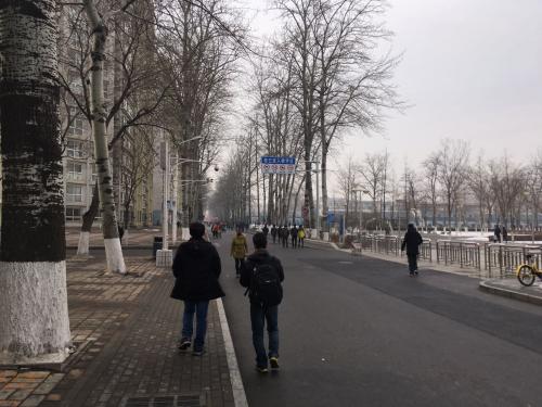
A typical road on a typical day in Beijing. The sky in Beijing is not blue due to the high amount of pollution mainly from industries and transportation. Let us protect our environment!
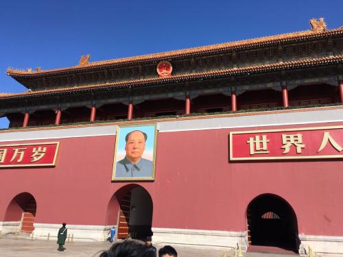
But fortunately the sky was blue during the day for excursion! As one of the destination, we visited the Palace Museum. Chinese students must know who this guy in the photo is!
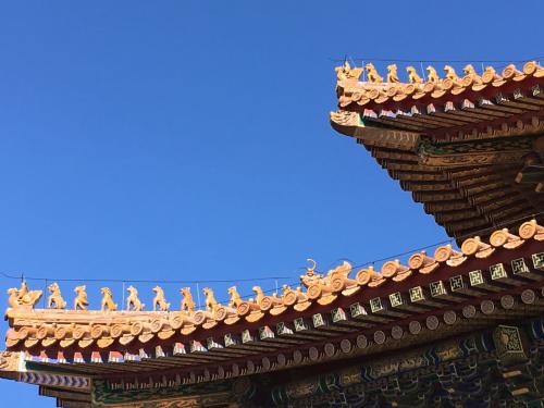
The roof of the temple is very artistic!
Before ending this post, I would like to thank the G-Safety program, which made this collaboration possible. I would also acknowledge Tanaka-sensei and Hirano-sensei for their guidance in my research. Also thanks to Kaneko-san for introducing me to this G-Safety program. Then the last but not the least, I would like to thank Miura-sensei and his lab members who have provided me the opportunity to learn something new.
And finally I would like to close this post with a quote:
For young researchers, don’t be too focused on your field. You should read other field’s literature, hear and discuss with other field’s researchers. Maybe the idea will come from other fields.
- Prof. Jean-Pierre Sauvage
(Nobel Laureate in Chemistry 2016)
at the Nobel Prize Dialogue Tokyo 2017: The Future of Intelligence
(Nobel Laureate in Chemistry 2016)
at the Nobel Prize Dialogue Tokyo 2017: The Future of Intelligence


No comments:
Post a Comment